Electron beam guns, often referred to as e-beam guns, are essential devices used to generate focused streams of electrons. These beams serve critical functions in scientific research, precision imaging, material processing, and semiconductor fabrication. As demand grows for nanotechnology and advanced materials, understanding how e-beam gun work and what components they include becomes vital for engineers, researchers, and manufacturers alike.
E-beam gun operate in high-vacuum environments and across a wide energy range—from a few keV (kiloelectron volts) up to several hundred keV or more. This flexibility allows them to be used in various domains, including electron microscopes, semiconductor lithography, and radiation curing. Their operational capacity can be tuned to suit delicate surfaces or penetrate dense substrates, depending on industrial needs.
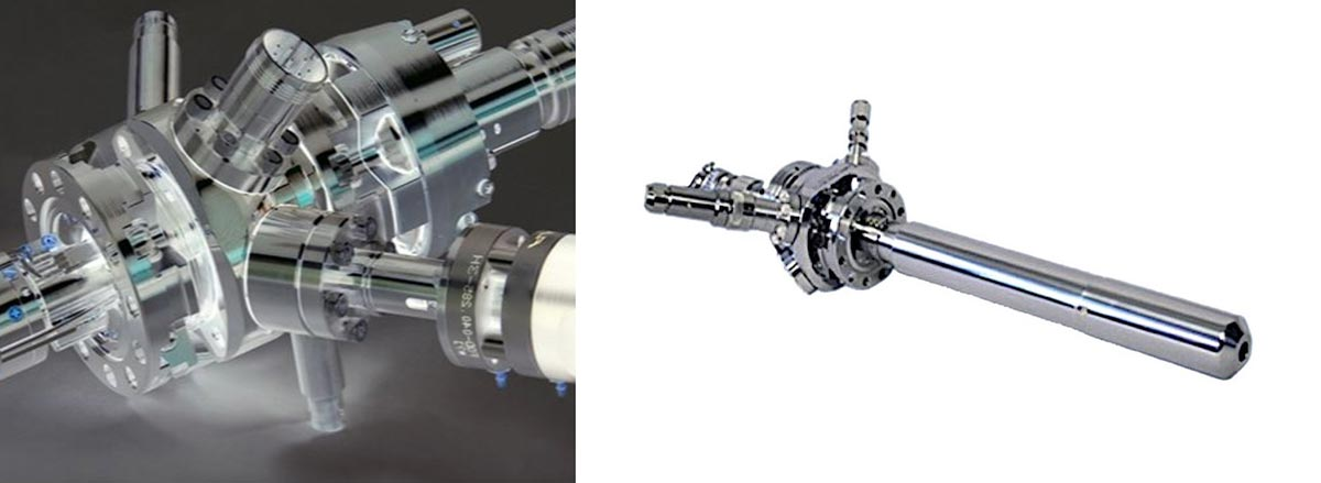
To understand how an electron beam is produced, it’s necessary to dissect its core components. Each part contributes to shaping, accelerating, and directing the electrons with extreme precision.
The cathode is the electron emitter and the starting point of the beam. It can be a thermionic emitter (using heat), a field emitter (using electric fields), or a photoemitter (using light). The efficiency and longevity of the beam heavily depend on the type of cathode material used.
The anode is positively charged and positioned near the cathode. It pulls emitted electrons forward and accelerates them. The energy of the beam is directly influenced by the voltage between the cathode and anode.
These are magnetic or electrostatic lenses that focus and direct the beam. Much like glass optics focus light, electron optics manage beam shape and clarity. Critical components include the Wehnelt cylinder, deflectors, and focusing coils.
Beam energy determines how deep electrons can penetrate a material. High-energy beams are useful for material modification, while lower-energy beams suit surface imaging or thin-film deposition.
Emission current controls beam brightness. A steady current is ideal for processes like e-beam welding or evaporation. Variations in current can affect uniformity in thin film coatings or microfabrication.
The spot size—the width of the beam—impacts resolution and material interaction. Smaller spots offer higher resolution, while wider beams cover larger areas. Beam divergence describes how much the beam spreads out after leaving the gun, which is minimized for precise targeting.
Some advanced systems include a zoom lens setup that allows the user to adjust focus dynamically, essential for applications like 3D printing with electron beams. Rastering or beam scanning moves the beam across a target in a controlled pattern, a fundamental requirement in semiconductor lithography and surface treatment.
Different operational needs require different gun types:
These rely on heating elements, typically tungsten, to emit electrons. They're widely used in CRTs and entry-level SEMs.
These use a high-voltage electric field for emission. Their high brightness and small spot size make them ideal for nanotechnology research and high-resolution imaging.
Operate without heat, often used in X-ray tubes, gas discharge tubes, and compact vacuum devices.
Specialized for signal amplification, these are commonly seen in mass spectrometers and photomultiplier tubes.
E-beam guns require an ultra-high vacuum (UHV) to prevent electron scattering. Systems include:
Without these, electron paths would become unstable, reducing beam precision.
E-beam lithography allows manufacturers to etch patterns at the nanoscale. Electron beams interact with resist-coated wafers, enabling the production of microchips, processors, and memory devices with extraordinary accuracy.
Used in both transmission (TEM) and scanning electron microscopes (SEM), electron guns provide the beams necessary to visualize atomic structures, cellular components, and materials science samples.
In vacuum deposition systems, e-beam guns heat metals to evaporate them, forming ultra-thin films on surfaces. This is commonly used in optics, solar cells, and hard coatings.
E-beam sterilizers kill bacteria and viruses on medical instruments, gloves, and packaging by penetrating them with ionizing radiation—clean, fast, and without residue.
Electron beams can melt metal powders in a controlled fashion to build complex parts layer by layer, especially in aerospace and medical implants.
Modern e-beam systems include automated control software, allowing remote operation, data logging, and dynamic tuning of beam parameters. Some systems feature modular designs with replaceable cathodes, beam conditioning optics, and spare firing units, ensuring low downtime and high adaptability across applications.
Electron beams are directed using electromagnetic coils or plates that deflect the path based on real-time inputs. This ensures micron-level accuracy.
Regular vacuum checks, emitter replacement, and calibration of optics ensure optimal performance and long system life.
They are compatible with a wide variety of metals, ceramics, and even polymers—depending on beam energy and environmental setup.
E-beam guns are a cornerstone of high-precision industries. Whether you're etching nanoscale chips, sterilizing medical tools, or exploring atomic structures, these electron beam systems offer unmatched accuracy, efficiency, and flexibility. With continuous advancements in beam control, emission sources, and integration with AI-driven systems, the future of e-beam technology is brighter—and sharper—than ever.